MIT researchers have developed a new artificial intelligence model capable of classifying and quantifying atomic-scale defects in materials without the need for invasive or destructive testing. By analyzing data from noninvasive neutron-scattering techniques, the model provides a precise way to measure defects that are intentionally introduced to enhance the strength, conductivity, and energy-conversion efficiency of materials like semiconductors and solar cells.
A New Paradigm in Defect Science
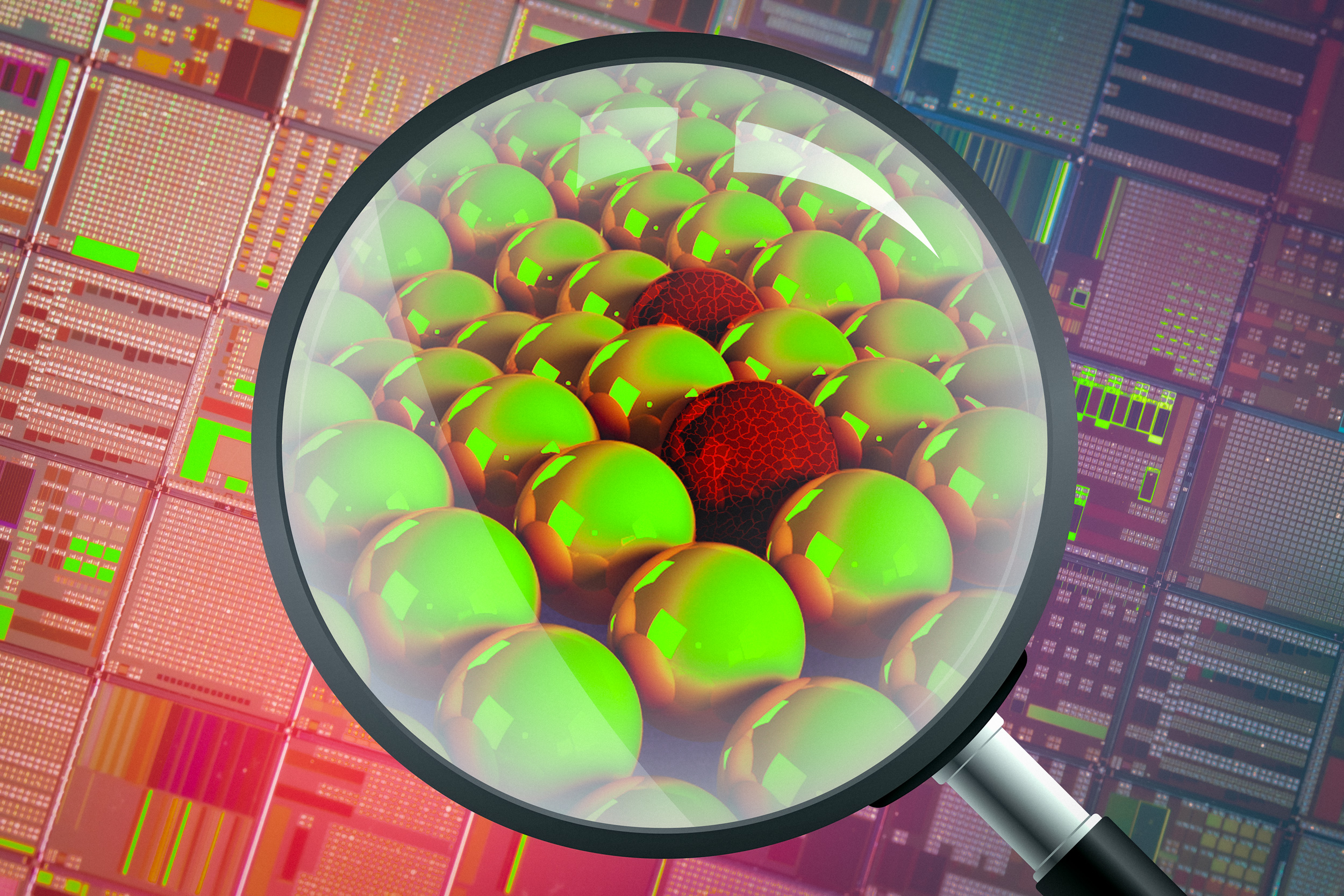
In materials science, defects are often intentionally tuned to improve product performance. However, accurately measuring these defects in finished products has historically been a significant challenge. Conventional methods, such as X-ray diffraction or transmission electron microscopy, are often limited in scope, require destructive sampling, or cannot simultaneously identify multiple types of defects.
As senior author and associate professor of nuclear science and engineering Mingda Li explains, existing techniques often provide only a partial view of the material. "Each technique can only see part of it," Li says. "We need better ways of getting the full picture of defects, because we have to understand them to make materials more useful."
Training the AI Model
To build the model, the research team created a computational database of 2,000 semiconductor materials. They used a neutron-scattering technique to measure the vibrational frequencies of atoms in both doped and undoped samples. By training the model on this data, the researchers created a system that leverages a multihead attention mechanism—similar to the technology used in ChatGPT—to extract differences in data and predict the types and concentrations of dopants present.
The resulting model is capable of detecting up to six different types of point defects simultaneously, even at concentrations as low as 0.2 percent. Lead author Mouyang Cheng notes that this level of detection was previously considered impossible, stating, "For conventional techniques without machine learning, detecting six different defects is unthinkable."
Future Applications and Scalability
While the current model relies on neutron-scattering data, the researchers are already looking toward more accessible applications. Because neutron-scattering facilities are not always readily available for rapid quality control, the team is working to adapt the model for use with Raman spectroscopy, a widely used technique that measures the scattering of light.
The researchers believe this work represents a significant shift in how engineers can monitor material quality. By moving beyond the "guessing game" of defect estimation, this AI-driven approach offers a more precise way to ensure that materials meet performance standards. The study, which was supported by the Department of Energy and the National Science Foundation, appears in the journal Matter.
Comments (0)
to join the discussion
No comments yet
Be the first to share your thoughts!